General Description
The Evaluation Board user guide describes the operational use of the RTQ2522A evaluation board as a reference design for demonstration and evaluation of the RTQ2522A, an ultra-low dropout (LDO) linear regulator with soft-start.
Included in this user guide are setup and operating instructions, thermal and layout guidelines, a printed circuit board (PCB) layout, a schematic diagram, and a bill of materials (BOM). For more detail information, please refer to the RTQ2522A datasheet
Performance Specification Summary
Summary of the RTQ2522A Evaluation Board performance specificiaiton is provided in Table 1. The ambient temperature is 25°C.
Table 1. RTQ2522A Evaluation Board Performance Specification Summary
|
Specification
|
Test Conditions
|
Min
|
Typ
|
Max
|
Unit
|
|
Input Voltage Range
|
|
VOUT + Vdrop
|
1.1
|
5.5
|
V
|
|
VBIAS Pin Voltage
|
|
2.7
|
--
|
5.5
|
V
|
|
Output Voltage Range
|
Vin = 5V, IOUT = 2A
|
0.8
|
0.8
|
3.6
|
V
|
|
Line Regulation
|
VOUT (normal) + 0.3V ≤ VIN ≤ 5.5V
|
--
|
0.03
|
--
|
%/V
|
|
Load Regulation
|
50mA ≤ IOUT ≤ 2A
|
--
|
0.09
|
--
|
%/A
|
|
VIN Dropout Voltage
|
IOUT = 2A,
VBIAS – VOUT (normal) ≥ 3.25V
|
--
|
100
|
150
|
mV
|
|
VBIAS Dropout Voltage
|
VOUT = 80% x VOUT (normal)
|
--
|
1.55
|
1.8
|
V
|
Power-up Procedure
Suggestion Required Equipments
- RTQ2522A Evaluation Board
- DC power supply capable of at least 5.5V and 2A
- Electronic load capable of 2A
- Function Generator
- Oscilloscope
Quick Start Procedures
The Evaluation Board is fully assembled and tested. Follow the steps below to verify board operation. Do not turn on supplies until all connections are made. When measuring the output voltage ripple, care must be taken to avoid a long ground lead on the oscilloscope probe. Measure the output voltage ripple by touching the probe tip and groundring directly across the last output capacitor.
Proper measurement equipment setup and follow the procedure below.
1) With power off, connect the input power supply to VIN and GND pins.
2) With power off, connect the electronic load between the VOUT and nearest GND pins.
3) Turn on the power supply at the input. Make sure that the input voltage does not exceeds 6V on the Evaluation Board.
4) Check for the proper output voltage using a voltmeter.
5) Once the proper output voltage is established, adjust the load within the operating ranges and observe the output voltage regulation, quiescent current, dropout voltage, PSRR, noise and other performance.
Detailed Description of Hardware
Headers Description and Placement
Carefully inspect all the components used in the EVB according to the following Bill of Materials table, and then make sure all the components are undamaged and correctly installed. If there is any missing or damaged component, which may occur during transportation, please contact our distributors or e-mail us at evb_service@richtek.com.
Test Points
The EVB is provided with the test points and pin names listed in the table below.
|
Test Point/
Pin Name
|
Function
|
|
VIN
|
Supply input pin.
|
|
VOUT
|
Output of the regulator.
|
|
PG
|
Power good sense pin.
|
|
VBIAS
|
Input pin of bias voltage.
|
|
EN
|
Enable sense pin.
|
|
GND
|
System ground pin.
|
|
SS
|
Soft-start capacitor waveform sense pin.
|
|
ENABLE
|
User can decide EN pin connected to high or low.
|
|
BIAS-EN/VIN-EN
|
Decision of EN pin pull-high voltage source.
|
|
BIAS-PG/VOUT-PG
|
Decision of PG pull-high voltage source.
|
Bill of Materials
|
VIN = 1.1V to 6.5V, VOUT = 0.8V to 5.5V, IOUT = 2A
|
|
Reference
|
Count
|
Part Number
|
Value
|
Description
|
Package
|
Manufacturer
|
|
U1
|
1
|
RTQ2522AGQW(2)
|
RTQ2522A
|
LDO
|
WDFN-10L 3x3
|
RICHTEK
|
|
C1
|
1
|
TMK212BJ475KG-T
|
4.7μF
|
Capacitor, ceramic,
25V, X5R
|
0805
|
TAIYO YUDEN
|
|
C3
|
1
|
GRM21BR71A106KE51L
|
10μF
|
Capacitor, ceramic,
10V, X7R
|
0805
|
MURATA
|
|
CBIAS
|
1
|
0805B105K250CT
|
1μF
|
Capacitor, ceramic,
25V, X7R
|
0805
|
WALSIN
|
|
CSS
|
1
|
0603B102K500CT
|
1nF
|
Capacitor, ceramic,
50V, X7R
|
0603
|
WALSIN
|
|
R1, R5
|
2
|
WR06X000 PTL
|
0
|
Resistor, chip
|
0603
|
WALSIN
|
|
REN1, REN2, RPG1, RPG2
|
4
|
WR06X1003FTL
|
100k
|
Resistor, chip
|
0603
|
WALSIN
|
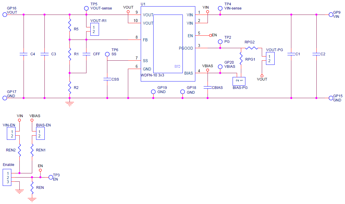
Typical Applications
EVB Schematic Diagram
1. The capacitance values of the input and output capacitors will influence the input and output voltage ripple.
2. MLCC capacitors have degrading capacitance at DC bias voltage, and especially smaller size MLCC capacitors will have much lower capacitance.
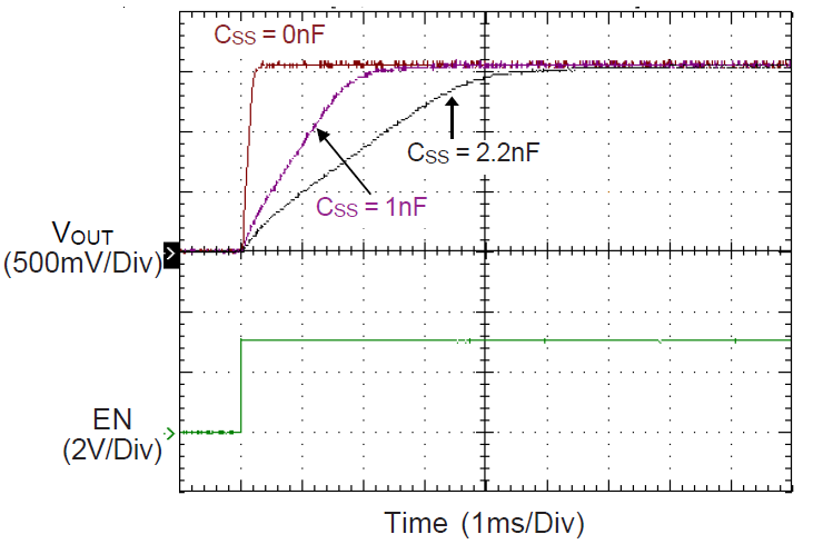
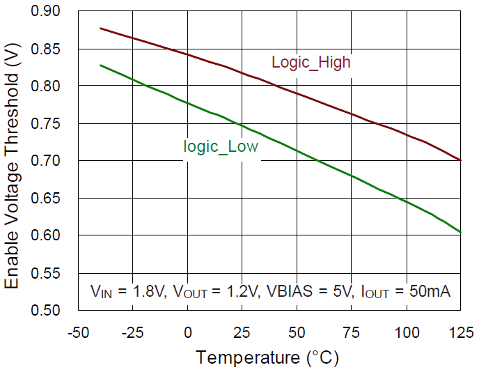
Measure Result
|
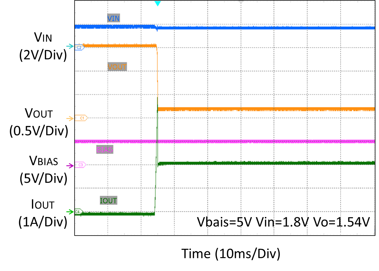
Power Up Response
|
Enable Voltage Threshold vs. Temperature
|
|
|
|
|
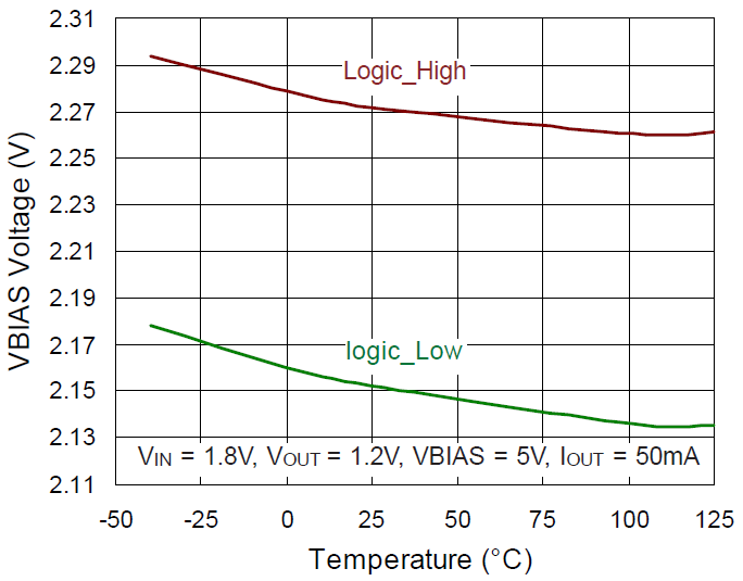
VBIAS Voltage UVLO vs. Temperature
|
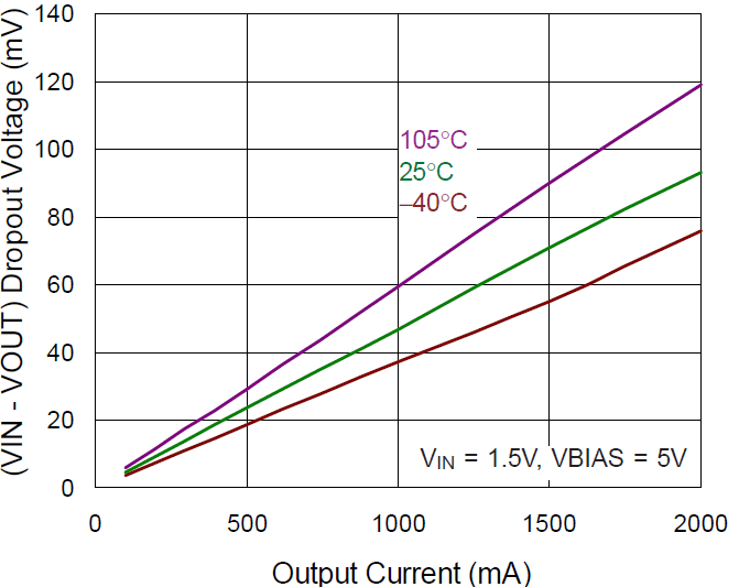
Dropout Voltage vs. Output Current
|
|
|
|
|
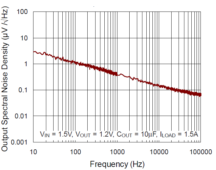
Output Spectral Noise Density
|
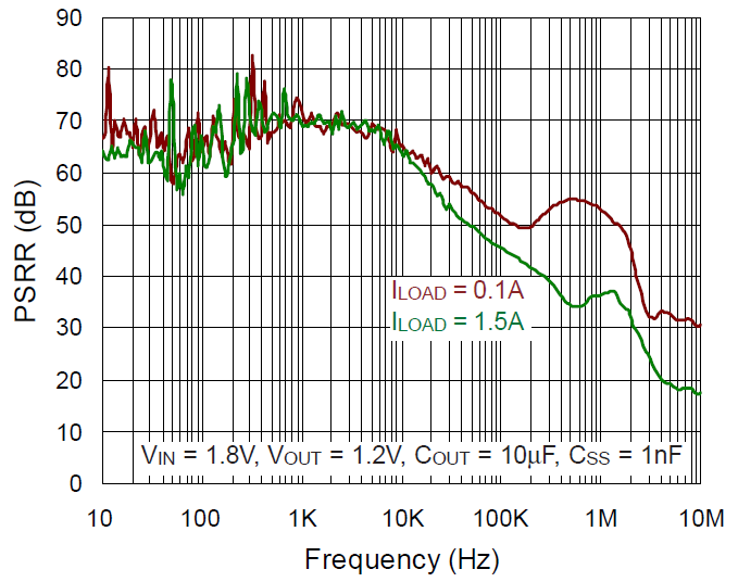
VIN PSRR vs. Frequency
|
|
|
|
|
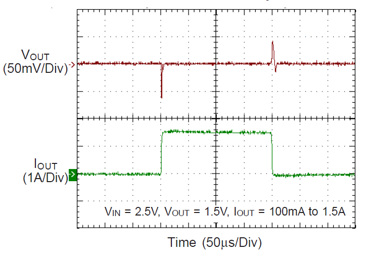
Load Transient Response
|
OCP
|
|
|
|
|
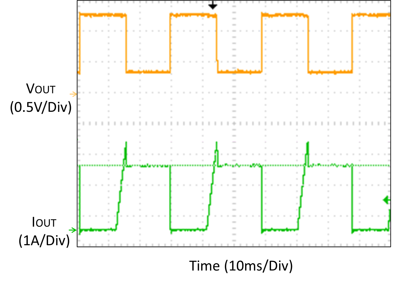
Short Protection
|
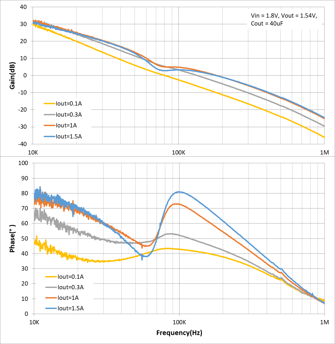
Bode Plot
|
|
|
|
Note: When measuring the input or output voltage ripple, care must be taken to avoid a long ground lead on the oscilloscope probe. Measure the output voltage ripple by touching the probe tip directly across the output capacitor.
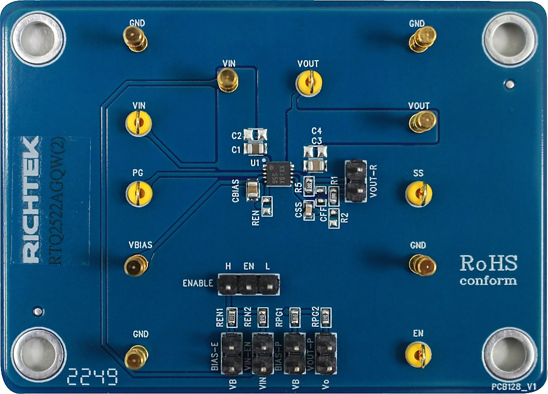
Evaluation Board Layout
Figure 1 to Figure 4 are RTQ2522A Evaluation Board layout. This board is constructed on four-layer PCB, outer layers with 1 oz. Cu and inner layers with 1 oz. Cu.
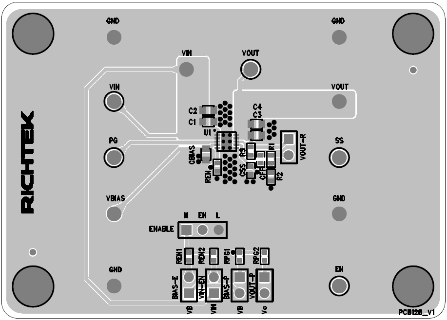
Figure 1. Top View (1st layer)
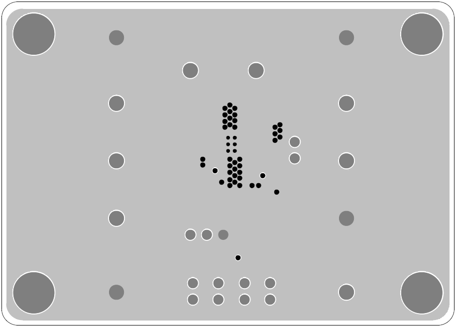
Figure 2. PCB Layout—Inner Side (2nd Layer)

Figure 3. PCB Layout—Inner Side (3rd Layer)
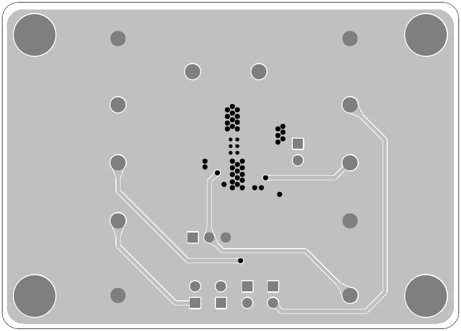
Figure 4. Bottom View (4th Layer)